Aenean ornare velit lacus, ac varius enim lorem ullamcorper dolore aliquam.
Silicon-based cells are currently the most popular solar cells in use because of their complete knowledge of the fabrication techniques and comparatively good energy conversion efficiencies in the range of 20-25%. About 85% of all the installed solar cells in the world are made of Silicon. However, the cost of a Silicon-based solar cell is very high due to the high cost of Silicon wafers used in the fabrication and due to the high fabrication cost.
Low-cost solar cells can be produced using comparatively cheaper materials and with lower fabrication costs by employing thin film technology as it uses fewer materials. There are different types of thin film solar cell materials available like Cadmium Telluride (CdTe), Copper-Indium-Gallium-Diselenide (CIGS), and Gallium-Arsenide (GaAs) with proven efficiencies of about 12-28 % but these elements cause environmental pollution and are also scarcely available. The solution to these problems is earth-abundant, eco-friendly, Copper Zinc Tin Sulfide (CZTS), also known as Kesterite which is a quaternary p-type semiconductor material with a band gap of about 1.5 eV, and high absorption coefficient of 104 cm-1.
In this project, Kesterite was synthesized using two sequential deposition techniques namely the Thermal Evaporation System, and the Magnetron Sputtering System. The architecture of the solar cell was finalized for the absorber layer, buffer layer, window layer, and top contact layer followed by optimizing the deposition parameters for each of these coatings. Finally, a proposed design of a PV module incorporating stacks of individual cells was proposed and tested for its performance.
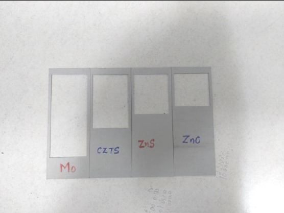
Masking of individual layers is necessary to prevent any problems arising while synthesizing CZTS solar cells(short circuit between top contact and bottom contact) and also to be able to extract the lead wires from appropriate layers. These masks were made through laser cutting and were tested rigorously for optimal deposition parameters of each layer.. For the development of the PV module, the size was chosen based on calculations of the power output required and the optimal heat dissipation characteristics.
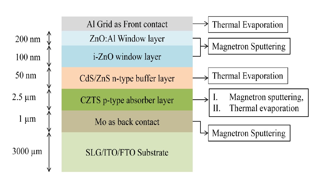
The thin-film kesterite-based solar cell follows a multi-layered device architecture, as illustrated in the Figure. The substrate comprises Soda Lime Glass (SLG), Indium Tin Oxide (ITO), and Fluorine Tin Oxide (FTO). Mo serves as the back contact for the CZTS-based thin-film solar cell. The absorber layer (p-type) utilizes CZTS due to its high absorption coefficient (104 cm-1) and a direct band gap of approximately 1.5eV. The n-type buffer layer employs CdS or ZnS for compatibility with p-type CZTS. The window layer incorporates Intrinsic Zinc Oxide (i-ZnO) and Aluminum-doped ZnO (ZnO: Al), while the top contact utilizes cost-effective aluminum for good electrical conductivity.
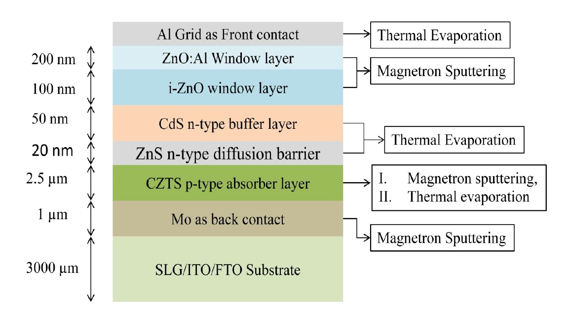
There was a problem that was noticed in the initial architecture which caused the formation of a transistor instead of a solar cell. It was observed that CdS was being diffused into the CZTS layer. To avoid this, a new n-type diffusion barrier was proposed and the architecture of the solar cell was modified as shown in the figure. ZnS was also synthesized as part of the project and was deposited through the Thermal Evaporation System.
Mo was coated on (50*50) mm2 square SLG. Then after that, Mo/Zn/Sn/Cu by Thermal evaporation followed by Sulfurization. Then after that ZnS and CdS were done successfully. For coating of CZTS p-type absorber layer CZTS mask with utilization area of 4*4 cm2. The thickness calculation was done using a gravimetric method where high precision weight balance was used to measure the weight. gain by the substrate. After this sulfurization was done for this cell, where the sulfur powder amount was approx. 10gm for the sulfurization process and the set temperature (FT) was 450ᵒC. This was followed by the deposition of ZnS and CdS layers.
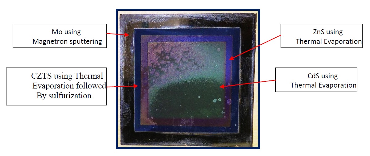
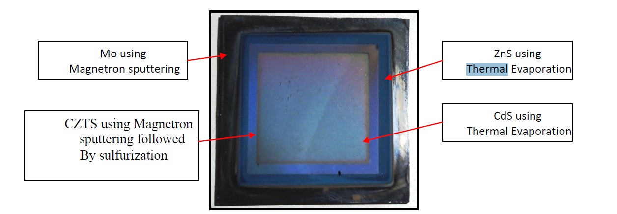
Compared to the above image, here the layers of Zn/Sn/Cu were deposited using Magnetron Sputtering instead of thermal evaporation system.
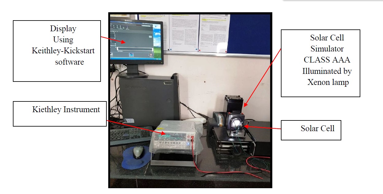
Both the thin film solar cells were tested at Dr. Babasaheb Ambedkar Marathwada University, Aurangabad (Physics Dept.) under the observation of Dr. Ramphal B. Sharma (Professor & Head of Dept.). In this test, a Class AAA solar cell simulator was used where the solar cell was placed in front of the solar simulator illuminated by a xenon lamp. Initally both the solar cells performed as a transistor and after the modification of architecture, a third solar cell was developed using just the TES method. The solar cell showed very high series resistance, resulting in an efficiency of about 1.08 %.
